https://habr.com/en/company/spbifmo/blog/487600/- ITMO University corporate blog
- Development for IOT
- Manufacture and development of electronics
- Offices of IT companies
- Physics
Today we’re taking a look at the Functional Materials and Devices of Optoelectronics Lab at
ITMO University, the equipment it houses, and the projects underway at the facility.
It is an international research facility located in the center of St. Petersburg. The staff is primarily occupied with the search for innovative materials (semiconductors, metals, and nanostructured oxides), and the
manufacturing of next-gen micro- and optoelectronic gadgets. Here we take a look at the
high-tech equipment it utilizes.
 © ITMO University
Much of the work being done has to do with energy-efficient LED lighting. This tech is currently in high demand, and generates a lot of interest among power grid operators. Students lovingly call it “The Romanov Laboratory” after its head —
Aleksey Romanov. This distinguished physicist with more than 300 scientific papers under his belt is currently the Dean of the university’s Laser Photonics and Optoelectronics department.
Equipment
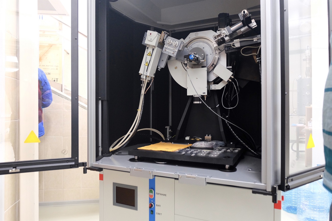
The lab is equipped with a DRON-8 X-ray diffractometer, manufactured by Russia’s own “Bourevestnik”.
It measures crystals and heterostructures’ X-ray diffraction — which is necessary to determine their mineral composition. It can also be used to apply heat to thin film semiconductors.

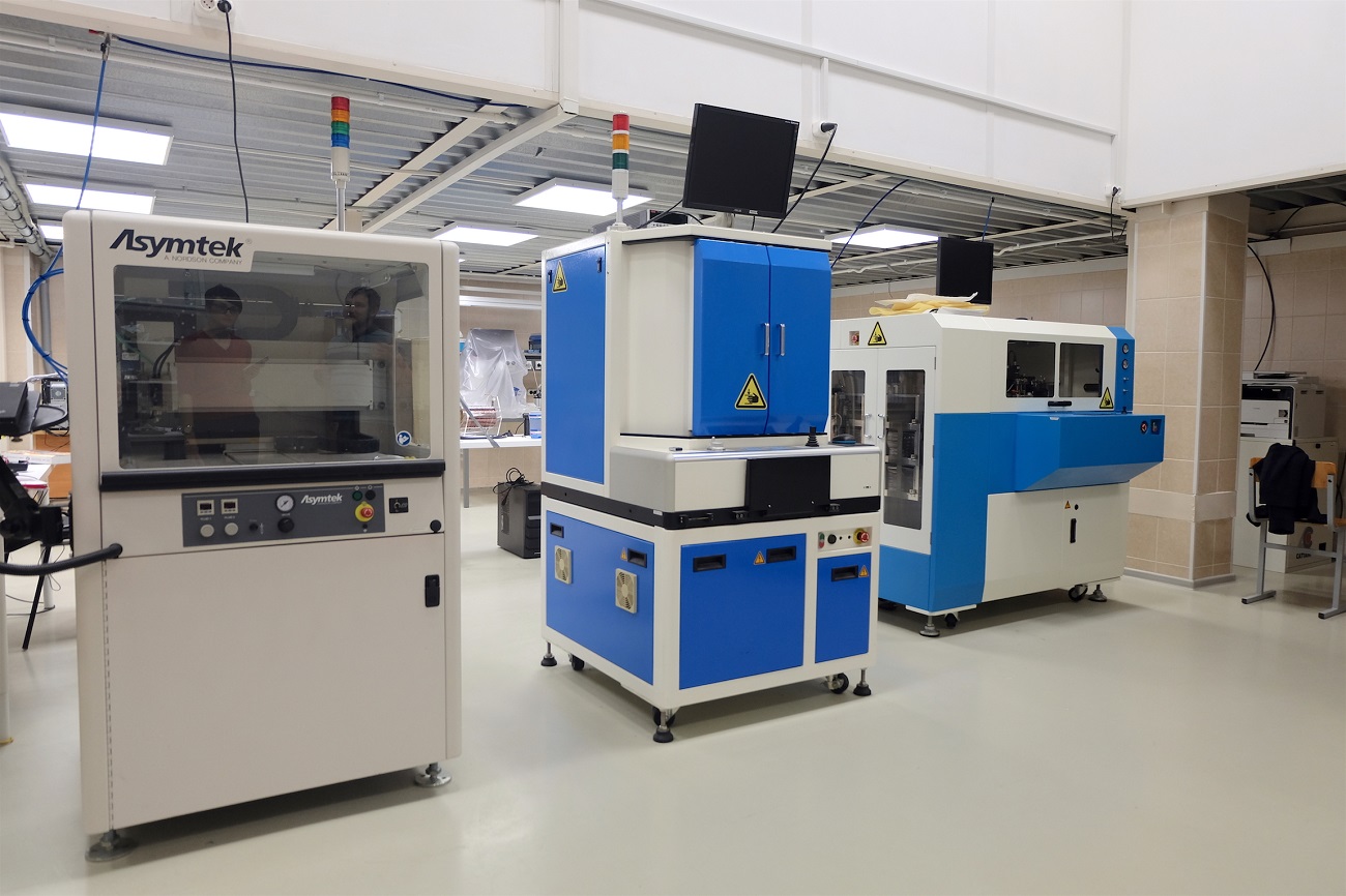
We use a number of small-scale industrial-grade machines to analyse, modify and sort LEDs.
On the left you can see the
Asymtek S-820 precision dispenser. It is an automated dispenser for viscous liquids. Such a tool is vital to ensure the LEDs we assemble are the colours we want them to be. Applying the wrong amount of phosphor during the manufacturing process can ruin the final product.

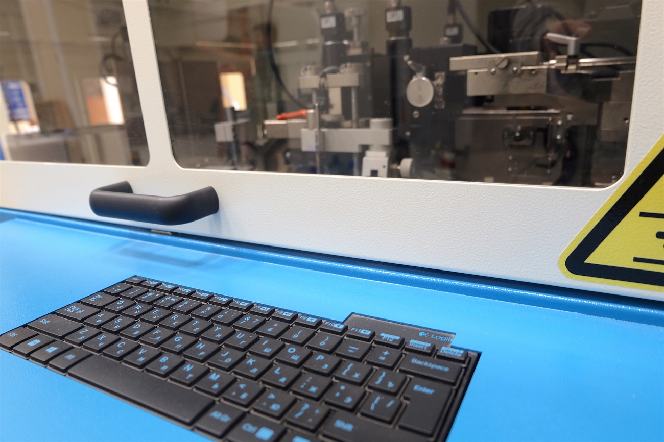
To the right of the dispenser is the machine we use to measure and store the electrical and spectral characteristics of a large number of LED chips. This data is needed for the purposes of quality control.

Here’s what the machine looks like on the inside:

The rightmost device in the
photo is used to sort the LEDs prior to their installation. It compiles all the LED measurements into a single file, assesses their quality and assigns them a numbered category (category 1 LEDs emit no light at all, while category 256 LEDs emit bright light strictly within the required spectral range).

Apart from the LEDs, the lab staff is also tasked with manufacturing semiconductors and heterostructures. The latter are created with molecular beam epitaxy on the RIBER MBE 49 machine located at the lab of one of our partners — Connector Optics LLC. To obtain oxide single crystals for wide-gap semiconductors, we use the domestically produced NIKA-3 crystal growth unit. The semiconductors we manufacture can be used in power relays, high-performance vertical lasers, ultraviolet detectors, and other products.
Projects
Our International Research centre is home to multiple theoretical and applied research projects.
We’re
developing new kinds of metal conductors. The alloys are heated, which redistributes their impurities, increasing the materials’ conductivity and strength. This research is being done in collaboration with the Ufa State Aviation Technical University. The lab is also developing photonic transceivers for use in high-bandwidth communication systems. The project is still in its early stages — once the necessary documentation is approved, work on the prototypes can commence.
Wide-gap semiconductors and low defect density nanostructures are also being actively worked on. These materials will enable the manufacturing of extremely energy-efficient devices. At the moment, no such technology is commercially available.
Our experts have already
developed ultraviolet LEDs capable of replacing legacy mercury-based products. The safer and more powerful alternative is expected to be applied in healthcare, water treatment and similar fields.
A different group of scientists from our lab is
working on the next generation of digital screens. The OLEDs of the future will take advantage of nanoparticles’ quantum properties to emit light without generating heat. There’s still work to be done before this invention can become commercially available — for now, the team is occupied with making sure it’s 100% safe.
Further reading:
